Product Description:
The Communication PCB Assembly is a highly specialized printed circuit board designed to meet the demanding requirements of modern communication infrastructure. Engineered with precision and advanced technology, this PCB assembly plays a crucial role in ensuring reliable and efficient performance in various communication systems. Featuring a minimum hole diameter of 0.1mm, the board allows for ultra-fine connections, making it ideal for high-density circuit designs and complex component placements that are common in communication equipment.
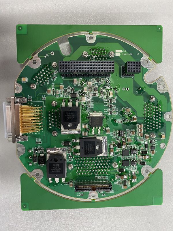
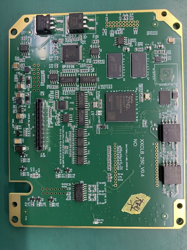
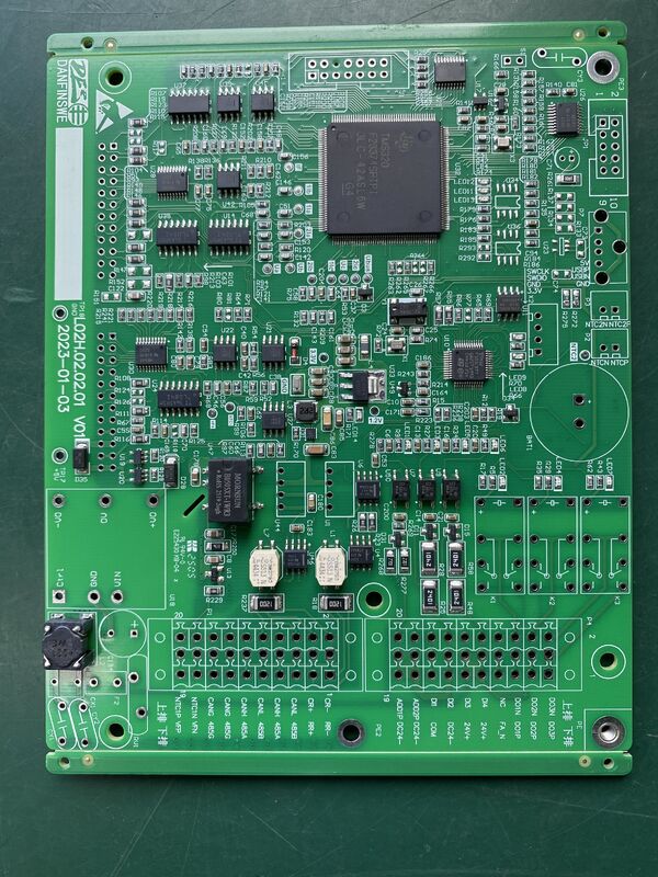
This PCB assembly is constructed with 6 layers, providing a robust and versatile platform for intricate routing and signal integrity. The multi-layer design enhances the board’s capability to handle high-speed data transmission and complex communication protocols, which are essential in today’s fast-evolving communication infrastructure. The six layers enable designers to optimize power distribution, signal isolation, and EMI shielding, thereby improving overall system performance and reliability.
One of the standout features of this Communication PCB Assembly is its use of high Tg materials, specifically Tg170 and Tg180. These high glass transition temperature materials ensure that the PCB maintains its mechanical strength and electrical properties under elevated thermal conditions. This is particularly important in communication infrastructure where devices often operate under continuous high temperatures due to heavy data traffic and prolonged usage. The high Tg materials contribute to the board’s durability, reducing the risk of warping and failure, thus extending the lifespan of the communication devices.
The board thickness ranges from 0.2mm to 6mm, offering flexibility to accommodate different design requirements and mechanical constraints. Thinner boards are suitable for compact and lightweight devices, while thicker boards provide enhanced mechanical strength and thermal management. This wide range of thickness options allows manufacturers to tailor the PCB assembly to specific applications within the communication infrastructure sector, whether it be for handheld devices, base stations, or data centers.
In addition to its structural and material advantages, the Communication PCB Assembly is available with various solder mask colors, including blue, green, and others. The solder mask not only protects the copper circuitry from oxidation and contamination but also improves the aesthetic appeal and facilitates easier inspection and assembly processes. The availability of different solder mask colors allows customization according to customer preferences and industry standards.
Another critical aspect of this product is the incorporation of thick copper layers, which significantly enhance the current-carrying capacity and heat dissipation capabilities of the PCB. Thick copper is vital in communication infrastructure applications where high power delivery and efficient thermal management are required to maintain signal integrity and prevent overheating. The use of thick copper layers ensures that the PCB can handle demanding electrical loads and maintain stable operation under rigorous conditions.
Overall, the Communication PCB Assembly is a high-performance solution tailored for the communication infrastructure industry. Its combination of fine hole diameter, multi-layer construction, high Tg materials, customizable thickness, and solder mask options, along with the integration of thick copper, makes it an excellent choice for manufacturers seeking reliability, durability, and superior electrical performance. This PCB assembly supports the advancement of communication technologies by providing a solid foundation for devices that connect people and systems globally.
Whether used in telecommunications equipment, networking devices, or other communication infrastructure components, this PCB assembly ensures optimal performance and longevity. Its design and material choices reflect a deep understanding of the challenges faced in the communication sector, making it a trusted component in the development of next-generation communication solutions.
Features:
- Product Name: Communication PCB Assembly
- PCB Layers: 6 Layers
- PCB Quality System: ROHS compliant
- Board Thickness: 0.2-6mm
- PCB Board Type: HDI PCB
- Features thick copper for enhanced conductivity
- Includes surge protection for improved reliability
- Advanced surge protection technology to safeguard components
Technical Parameters:
| Product Name |
Communication PCB Assembly |
| Application Field |
5G Communication |
| PCB Quality System |
ROHS |
| PCB Board |
HDI PCB |
| Minimum Hole Diameter |
0.1mm |
| Surface Finishing |
ENIG, HASL Lead Free |
| Impedance Control |
Yes |
| Communication PCB |
High Tg170 and High Tg180 |
| Board Thickness |
0.2-6mm |
| Via Type |
Through Hole, Blind, Buried |
| Special Features |
Thick copper, Heavy Current |
Applications:
The Communication PCB Assembly is an essential component designed for a wide range of communication devices and systems. Featuring a robust 6-layer PCB structure, this assembly supports complex circuit designs necessary for high-speed data transmission and reliable communication networks. Its high Tg170 and high Tg180 materials ensure exceptional thermal stability and mechanical strength, making it suitable for demanding environments where temperature fluctuations and mechanical stresses are common.
This product is particularly ideal for use in telecommunications infrastructure, including base stations, routers, switches, and signal processing units. The thick copper layers integrated into the PCB enhance electrical conductivity and improve current carrying capacity, which is crucial for maintaining signal integrity and reducing power loss in communication equipment. The repeated emphasis on thick copper underscores its importance in providing durability and performance reliability for critical communication applications.
In addition to telecommunications, the Communication PCB Assembly finds its application in data centers and network servers where high-speed and stable data transfer is paramount. The surface finishing options, including ENIG (Electroless Nickel Immersion Gold) and lead-free HASL (Hot Air Solder Leveling), provide excellent surface planarity and solderability, ensuring strong and reliable component bonding. This is particularly advantageous in automated assembly lines and for maintaining long-term operational consistency.
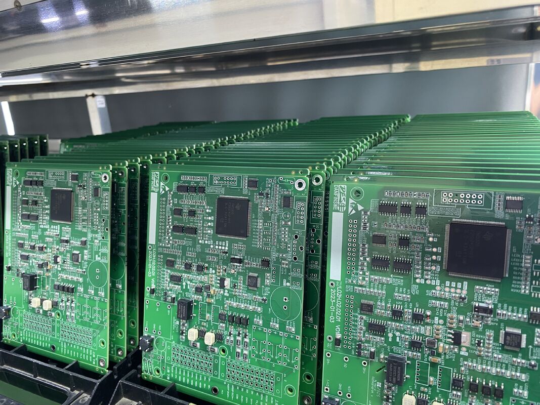
Furthermore, the product’s outer packaging in sturdy cartons guarantees safe transportation and handling, protecting the sensitive PCBs from physical damage and environmental factors during shipping and storage. This careful packaging approach highlights the manufacturer’s commitment to quality and customer satisfaction.
Overall, the Communication PCB Assembly is designed to meet the rigorous demands of modern communication technology. Its 6-layer design combined with thick copper layers, high Tg materials, and premium surface finishes make it an optimal choice for applications requiring high reliability, thermal endurance, and excellent electrical performance. Whether deployed in telecommunications, networking equipment, or data processing systems, this product ensures optimal communication efficiency and durability in various operational scenarios.
Customization:
Our Communication PCB Assembly offers advanced customization services tailored to meet the demanding requirements of 5G communication applications. As a reliable manufacturer, we ensure that each PCB assembly is crafted with precision, featuring a minimum hole diameter of 0.1mm and full impedance control to guarantee optimal signal integrity.
The product is securely packaged in a sturdy carton to protect against damage during transit. We also integrate surge protection features to safeguard your communication systems from voltage spikes and electrical surges, enhancing the reliability and longevity of your devices.
Choose our Communication PCB Assembly customization services for high-quality, durable solutions designed specifically for the evolving needs of the 5G communication sector, backed by expert surge protection technology from a trusted manufacturer.
Support and Services:
Our Communication PCB Assembly product is designed to meet the highest standards of quality and reliability in the telecommunications industry. We provide comprehensive technical support and services to ensure optimal performance and customer satisfaction.
Our technical support team is available to assist with installation, configuration, troubleshooting, and maintenance of the Communication PCB Assembly. We offer detailed product documentation, including datasheets, user manuals, and application notes to help you understand and utilize the product effectively.
In addition to support, we provide customization services to tailor the PCB assembly to your specific communication requirements. Our engineering experts work closely with your team to develop solutions that integrate seamlessly with your systems.
We also offer repair and refurbishment services to extend the lifecycle of your Communication PCB Assemblies, ensuring continued reliability and performance. Regular firmware and software updates are provided to keep your systems up to date with the latest features and security enhancements.
For any technical inquiries or service requests, our dedicated support team is committed to providing prompt and professional assistance to minimize downtime and maximize productivity.
Packing and Shipping:
Our Communication PCB Assembly products are carefully packaged to ensure maximum protection during transit. Each PCB assembly is placed in anti-static bags to prevent electrostatic discharge damage, followed by cushioning materials to absorb shocks and vibrations.
We use sturdy, high-quality boxes designed to withstand handling and environmental factors during shipping. Additionally, each package is clearly labeled with handling instructions and product information to facilitate smooth processing and delivery.
For shipping, we partner with reliable carriers to provide timely and secure delivery worldwide. Tracking information is provided for all shipments, allowing customers to monitor their orders until arrival.
We also offer customized packaging options upon request to meet specific requirements, ensuring that your Communication PCB Assembly products reach you in perfect condition.


 Your message must be between 20-3,000 characters!