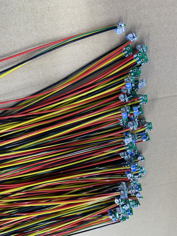
Product Description:
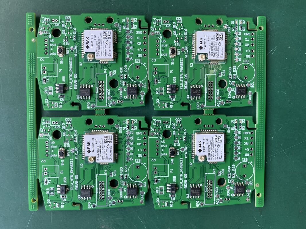
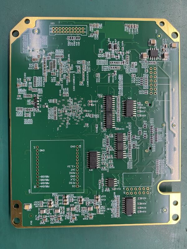
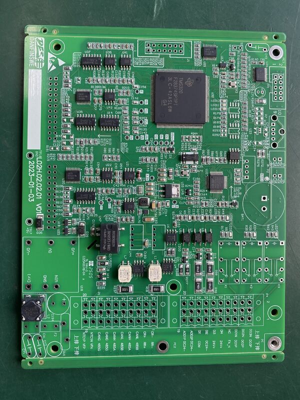
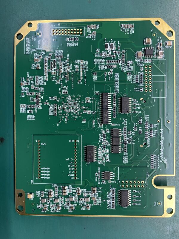
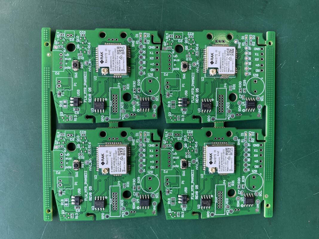
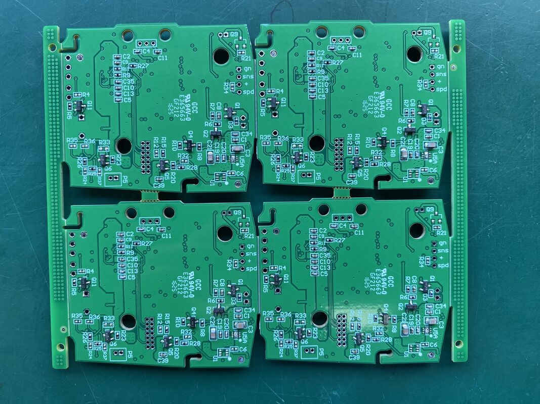
The Communication PCB Assembly is a highly specialized and meticulously engineered printed circuit board solution designed to meet the demanding requirements of modern communication systems. Manufactured with precision and care, this product offers a customized PCB size tailored specifically to the unique needs of each client, ensuring optimal performance and seamless integration into various communication devices and equipment. With a robust 6-layer design, the Communication PCB Assembly provides enhanced signal integrity, reduced electromagnetic interference, and improved overall reliability, making it an ideal choice for complex communication applications.
One of the standout features of this Communication PCB Assembly is its compliance with stringent quality standards, including the ROHS certification, which guarantees that the product is environmentally friendly and free from hazardous substances. This commitment to quality not only ensures safety and sustainability but also enhances the longevity and durability of the PCB assembly, making it suitable for long-term use in critical communication infrastructures.
The PCB assembly incorporates advanced impedance control, a crucial attribute for high-frequency communication circuits. Impedance control ensures that the electrical signals transmitted through the PCB maintain their integrity without distortion or loss, which is vital for maintaining clear and reliable communication channels. This feature is especially important in applications involving high-speed data transmission, where signal quality directly impacts performance.
In addition to its electrical performance characteristics, the Communication PCB Assembly is designed with a minimum hole diameter of 0.1mm, allowing for precise component placement and high-density circuitry. This fine detail supports the integration of complex components and supports miniaturization trends in communication device manufacturing. The ability to handle such small hole diameters demonstrates the manufacturer's advanced manufacturing capabilities and attention to detail.
Another critical aspect of this PCB assembly is its capability to handle heavy current loads safely and efficiently. Communication equipment often requires the management of significant electrical currents, and this PCB assembly is engineered to support heavy current applications without compromising performance or safety. The design incorporates features that minimize heat generation and ensure stable operation under high electrical stress, making it reliable for demanding communication environments.
Surge protection is an essential consideration in communication systems, where sudden voltage spikes can damage sensitive electronic components and disrupt service. The Communication PCB Assembly integrates surge protection mechanisms, safeguarding the circuitry against unexpected electrical surges. This protective feature extends the lifespan of the communication equipment and enhances overall system reliability, providing peace of mind to users and manufacturers alike.
As a trusted manufacturer in the PCB industry, the producer of this Communication PCB Assembly combines cutting-edge technology with rigorous quality control processes. Their expertise in producing customized PCB solutions ensures that every assembly meets precise specifications and performance criteria. By prioritizing innovation, quality, and customer satisfaction, this manufacturer delivers a product that not only meets but exceeds industry standards.
In summary, the Communication PCB Assembly is a top-tier product designed for high-performance communication applications. Its customized size, 6-layer configuration, and advanced impedance control make it suitable for complex and high-frequency circuits. The ROHS certification underscores its commitment to environmental responsibility and safety. With a minimum hole diameter of 0.1mm, it supports intricate component layouts, while its heavy current handling capability and integrated surge protection ensure durability and reliability in demanding communication environments. Manufactured by a reputable and experienced producer, this PCB assembly stands out as a dependable choice for anyone seeking quality and performance in communication PCB solutions.
Features:
- Product Name: Communication PCB Assembly
- Impedance Control: Yes, ensuring signal integrity for communication infrastructure
- Solder Mask Color: Available in Blue, Green, and other colors
- Outer Package: Securely packed in Carton for safe transportation
- Specification: PCB Customized Size to meet specific project requirements
- PCB Quality System: Compliant with ROHS standards for environmental safety
- Designed to handle Heavy Current applications efficiently
- Ideal for use in Communication infrastructure projects requiring reliable performance
Technical Parameters:
| Product Name |
Communication PCB Assembly |
| Application Field |
5G Communication |
| PCB Quality System |
ROHS |
| Specification |
PCB Customized Size |
| Surface Finishing |
ENIG, HASL Lead Free |
| PCB Board |
HDI PCB |
| Outer Package |
Carton |
| Min Hole Diameter |
0.1mm |
| PCB Layers |
6 Layers |
| Via Type |
Through Hole, Blind, Buried |
Applications:
The Communication PCB Assembly is a highly specialized product designed to meet the demanding requirements of modern 5G communication systems. With precise impedance control, this PCB assembly ensures minimal signal loss and optimal transmission quality, which is critical in high-frequency communication applications. The ability to customize the PCB size allows manufacturers to tailor the assembly to specific device configurations, making it ideal for various communication equipment.
This product is particularly suited for scenarios involving heavy current applications, where thick copper layers are necessary to handle high power loads without compromising the board’s integrity or performance. The use of thick copper not only enhances the current-carrying capacity but also improves thermal dissipation, which is vital in maintaining stable operation in high-density communication modules. Such attributes make it an excellent choice for base stations, antennas, and other infrastructure components within the 5G communication field.
The Communication PCB Assembly incorporates advanced viatype technologies, including through hole, blind, and buried vias. These features enable complex multilayer circuit designs, allowing for compact and efficient layouts that optimize signal routing and reduce electromagnetic interference. This capability is essential for manufacturers who require high-density interconnections in compact devices without sacrificing reliability or performance.
In terms of packaging, the PCB assemblies are carefully packed in durable cartons to ensure protection during transportation and storage. This outer packaging safeguards the product from physical damage and environmental factors, preserving its quality until it reaches the manufacturer or end user.
Manufacturers engaged in producing 5G communication equipment will find this Communication PCB Assembly highly beneficial due to its robust design and superior electrical characteristics. Whether used in network infrastructure, communication terminals, or IoT devices, the assembly provides the reliability and performance necessary to support the next generation of wireless communication technologies.
In summary, the Communication PCB Assembly is designed for heavy current applications with thick copper layers, offers customizable sizes, and employs advanced viatype structures such as through hole, blind, and buried vias. Its impedance control ensures excellent signal integrity, making it an indispensable component for 5G communication solutions. The careful carton packaging further enhances its suitability for manufacturers aiming to deliver high-quality, durable communication products.
Customization:
Our Communication PCB Assembly product offers comprehensive customization services tailored to meet your specific requirements. With a board thickness range of 0.2-6mm and up to 6 layers, we ensure high-quality manufacturing that supports complex communication applications. As a trusted manufacturer, we specialize in heavy current designs incorporating thick copper layers to enhance conductivity and durability. Our PCBs feature precise impedance control to guarantee optimal signal integrity. Additionally, we provide options for high Tg170 and high Tg180 materials, ensuring excellent thermal performance and reliability. Whether you need customized layouts, materials, or specifications, our communication PCB assemblies are designed to deliver superior performance for your demanding projects.
Support and Services:
Our Communication PCB Assembly product is supported by a dedicated technical support team committed to ensuring optimal performance and reliability. We provide comprehensive services including design consultation, assembly process optimization, testing and inspection, and troubleshooting assistance. Our experts are available to guide you through the entire lifecycle of the product, from initial design and prototyping to mass production and maintenance. We also offer customization services to meet specific communication requirements and industry standards. With a focus on quality and efficiency, our technical support ensures your communication systems operate seamlessly and effectively in any environment.
Packing and Shipping:
Our Communication PCB Assembly products are carefully packaged to ensure maximum protection during transit. Each PCB assembly is securely placed in anti-static bags to prevent electrostatic discharge damage, followed by cushioning materials to absorb shocks and vibrations.
The packaged assemblies are then boxed in sturdy, double-walled cartons designed to withstand handling and environmental stress. For added safety, we include desiccant packs to control moisture and maintain product integrity.
We offer multiple shipping options to meet your delivery requirements, including standard ground, expedited air freight, and international shipping services. All shipments are tracked and insured to guarantee timely and safe arrival of your Communication PCB Assembly products.
Our logistics team coordinates closely with carriers to provide real-time updates and ensure compliance with all regulatory and customs requirements for seamless delivery worldwide.


 Your message must be between 20-3,000 characters!