Product Description:
The Communication PCB Assembly is a highly specialized printed circuit board designed to meet the demanding requirements of modern communication infrastructure. This product is engineered with a customized PCB size to accommodate various design specifications, ensuring a perfect fit for different communication devices and systems. Its versatility and robust construction make it an ideal choice for manufacturers and developers working on advanced communication solutions.
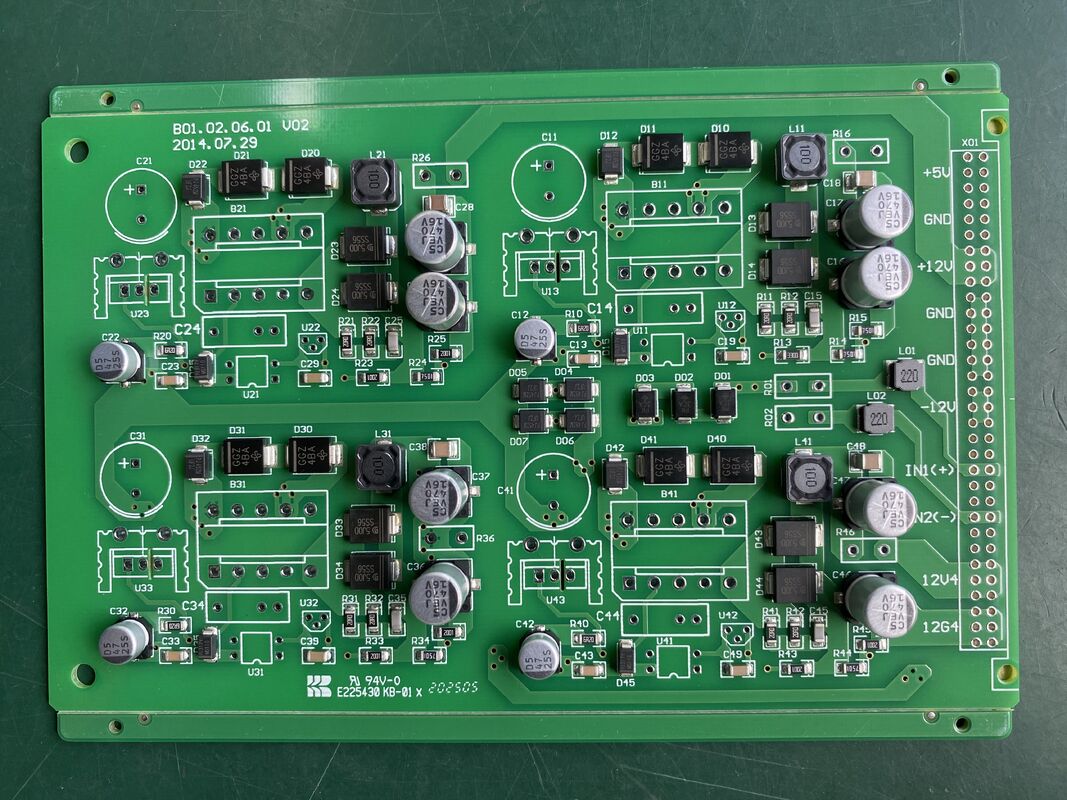
One of the standout features of this Communication PCB Assembly is its use of high Tg materials, specifically High Tg170 and High Tg180. These high glass transition temperature laminates provide excellent thermal stability and mechanical strength, essential for maintaining performance and reliability in environments with fluctuating temperatures and high operational stress. The High Tg materials ensure that the PCB can withstand the rigorous conditions often encountered in communication infrastructure applications, enhancing the longevity and durability of the final product.
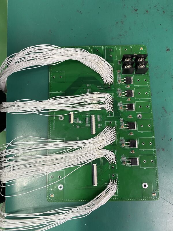
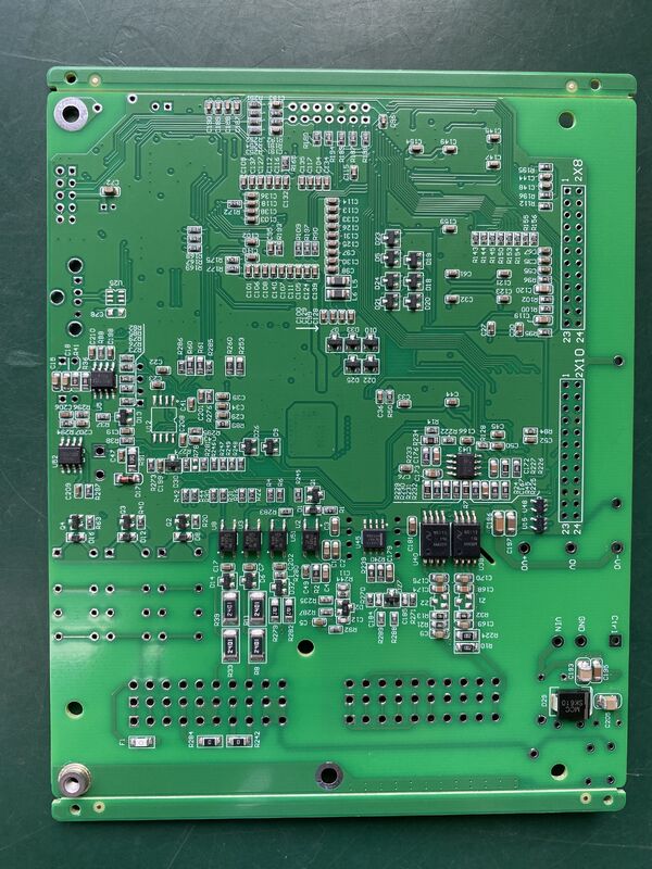
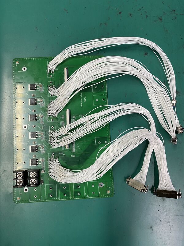
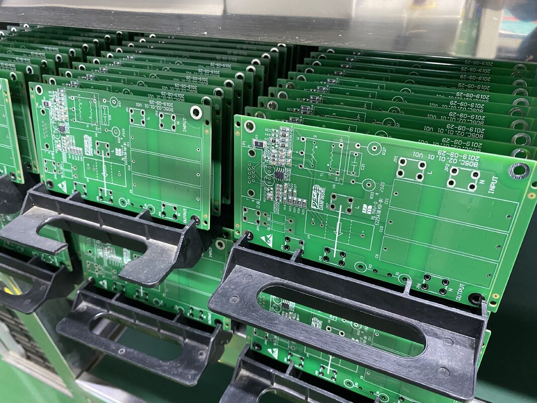
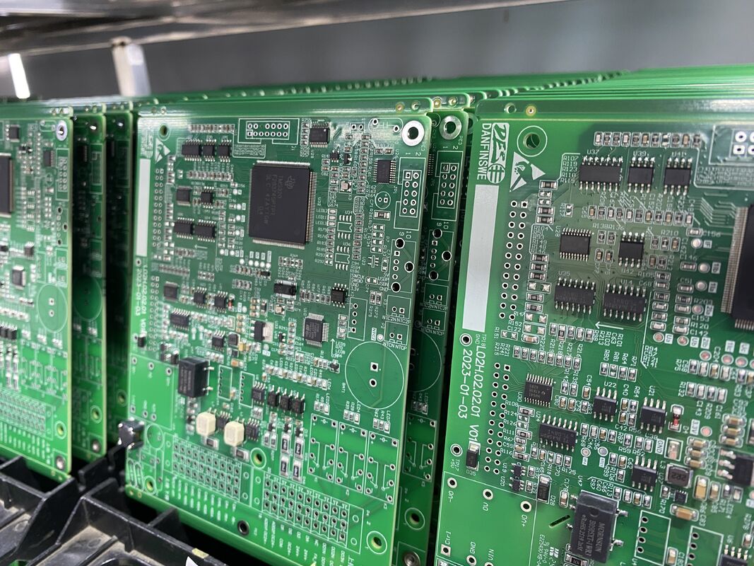
This assembly incorporates various via types, including through hole, blind, and buried vias, which contribute to its compact and efficient design. Through-hole vias facilitate strong mechanical connections and reliable electrical pathways, while blind and buried vias enable multi-layer PCB designs without compromising board space. This combination of via types allows for complex circuit layouts, supporting high-density interconnections essential for communication devices that require rapid and reliable data transmission.
Surface finishing is another critical aspect of the Communication PCB Assembly. It offers two high-quality surface finishing options: ENIG (Electroless Nickel Immersion Gold) and HASL (Hot Air Solder Leveling) Lead Free. ENIG provides a flat, solderable surface with excellent corrosion resistance and is ideal for fine-pitch components and high-frequency applications. HASL Lead Free, on the other hand, offers a cost-effective and environmentally friendly finishing option that maintains strong solderability and durability. Both finishes ensure the assembly is ready for efficient soldering during the manufacturing process and provide long-term protection against oxidation.
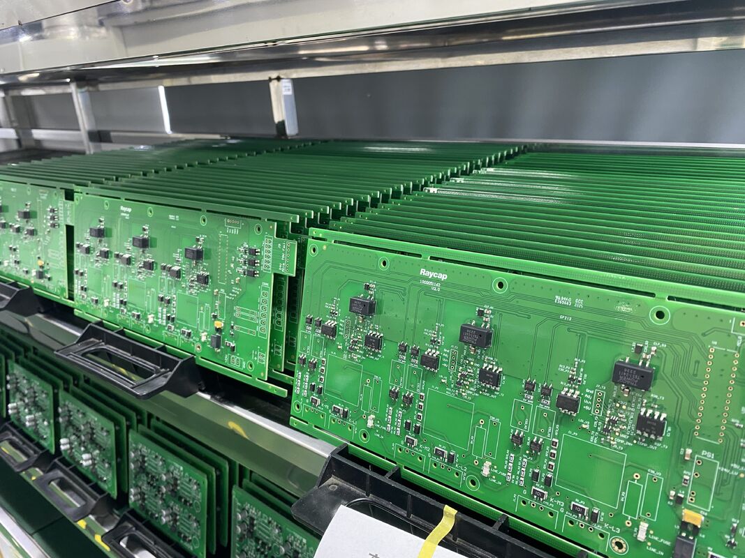
Thick copper layers are integral to this Communication PCB Assembly, enhancing its electrical performance and thermal management capabilities. Thick copper traces can carry higher current loads, reducing resistance and power loss, which is particularly vital in communication infrastructure where reliable signal integrity and power distribution are paramount. Moreover, the thick copper construction improves heat dissipation, preventing overheating and ensuring stable operation under heavy loads or continuous use.
In the context of communication infrastructure, the Communication PCB Assembly plays a crucial role in enabling high-speed data transfer and reliable connectivity. Its customized size and advanced material composition allow for seamless integration into various communication equipment, from base stations and routers to satellite and wireless communication devices. The assembly’s robust design and superior electrical properties contribute to the overall efficiency and performance of communication networks, supporting the ever-growing demand for faster and more reliable communication services.
Furthermore, the combination of thick copper layers and high Tg materials ensures that this PCB assembly can handle the rigorous electrical and thermal demands of modern communication systems. The use of multiple via types enhances signal routing flexibility and reduces electromagnetic interference, which is essential for maintaining clear and stable communication channels. The high-quality surface finishes protect the assembly from environmental factors, extending its service life and reducing maintenance costs.
In summary, the Communication PCB Assembly is a highly reliable and versatile solution tailored for the communication industry. Its customized PCB size, high Tg materials (High Tg170 and High Tg180), various via types (through hole, blind, buried), premium surface finishing options (ENIG and HASL Lead Free), and thick copper construction make it an excellent choice for supporting advanced communication infrastructure. This assembly not only meets the technical demands of modern communication devices but also ensures durability, efficiency, and long-term performance in a wide range of applications.
Features:
- Product Name: Communication PCB Assembly
- Board Thickness: 0.2-6mm, suitable for various applications
- Surface Finishing: ENIG and HASL Lead Free for enhanced durability and reliability
- Impedance Control: Yes, ensuring signal integrity for communication systems
- Specification: Customized PCB size to meet specific project requirements
- Designed to handle Heavy Current applications efficiently
- Supports Heavy Current transmission with Thick copper layers
- Thick copper layers provide excellent electrical performance and thermal management
Technical Parameters:
| Product Name |
Communication PCB Assembly |
| Impedance Control |
Yes |
| PCB Board |
HDI PCB |
| PCB Layers |
6 Layers |
| Communication PCB |
High Tg170 And High Tg180 |
| Min Hole Diameter |
0.1mm |
| Via Type |
Through Hole, Blind, Buried |
| PCB Quality System |
ROHS |
| Outer Package |
Carton |
| Application Field |
5G Communication |
| Manufacturer |
Experienced Manufacturer specialized in surge protection solutions |
Applications:
The Communication PCB Assembly is an essential component widely used in various communication devices and systems, designed to meet the rigorous demands of modern communication technology. With a board thickness ranging from 0.2mm to 6mm, this product offers exceptional versatility, allowing it to be integrated into a broad spectrum of applications, from compact handheld devices to large communication infrastructure equipment. The ability to accommodate through hole, blind, and buried vias ensures optimal connectivity and signal integrity, which is crucial in high-frequency communication environments.
One of the standout features of this Communication PCB Assembly is its support for very fine hole diameters, with a minimum hole size of just 0.1mm. This precision enables the creation of highly dense circuit layouts, essential for advanced communication devices that require miniaturization without compromising performance. Additionally, the use of high Tg170 and high Tg180 materials significantly enhances the thermal stability of the PCB, ensuring reliable operation under high-temperature conditions often encountered in communication systems.
This product is particularly well-suited for applications where surge protection is critical. Communication networks and devices are frequently exposed to electrical surges caused by lightning strikes, power fluctuations, or electromagnetic interference. The Communication PCB Assembly, with its robust design and thick copper layers, provides excellent surge protection capabilities. The thick copper ensures efficient current carrying capacity and heat dissipation, reducing the risk of damage due to sudden surges and maintaining the integrity of sensitive communication circuitry.
Typical application scenarios for the Communication PCB Assembly include telecommunications base stations, network routers, switches, and signal repeaters, where stable and uninterrupted signal transmission is mandatory. It is also ideal for satellite communication systems, fiber optic communication modules, and emergency communication equipment, where reliability and durability are paramount. In addition, this PCB assembly is used in industrial communication devices that operate in harsh environments, benefiting from its high Tg materials and surge protection features.
In summary, the Communication PCB Assembly combines advanced manufacturing techniques with high-performance materials to deliver a reliable and efficient solution for a wide range of communication applications. Its capabilities in handling through hole, blind, and buried vias, along with fine hole precision and thick copper layers, make it indispensable for ensuring surge protection and maintaining communication system stability across various demanding scenarios.
Customization:
Our Communication PCB Assembly product offers comprehensive customization services tailored to meet your specific needs. Manufactured under a strict ROHS quality system, our PCBs ensure environmentally friendly and reliable performance. We provide surface finishing options including ENIG and HASL Lead Free, guaranteeing excellent durability and conductivity.
Designed specifically for the 5G communication field, our PCBs support advanced applications requiring high-speed and stable connections. With a specification for customized PCB sizes, we cater to unique design requirements without compromising quality.
Additionally, our customized PCBs are engineered to handle heavy current loads efficiently, making them ideal for applications involving surge protection. Whether you need to protect sensitive components or ensure system stability under electrical surges, our communication PCBs deliver robust surge protection solutions.
Choose our customized Communication PCB Assembly services for superior quality, tailored specifications, and enhanced surge protection capabilities to support your advanced 5G communication projects.
Support and Services:
Our Communication PCB Assembly product is supported by a dedicated technical support team committed to ensuring optimal performance and reliability. We provide comprehensive services including design consultation, troubleshooting assistance, firmware updates, and maintenance guidance to help you maximize the functionality of your communication systems.
We offer tailored support solutions to address specific project requirements, including prototype development, testing, and quality assurance. Our experts are available to assist with integration challenges and to provide recommendations for enhancing signal integrity and overall system efficiency.
In addition, we provide extensive documentation and resources, including user manuals, installation guides, and FAQs, to facilitate smooth deployment and operation. Our commitment to continuous improvement ensures that you receive timely updates and enhancements aligned with the latest industry standards.
Whether you require on-site support, remote troubleshooting, or customized training sessions, our technical support and service teams are equipped to deliver responsive and effective solutions to meet your communication PCB assembly needs.
Packing and Shipping:
Our Communication PCB Assembly products are carefully packaged to ensure maximum protection during transit. Each PCB assembly is placed in anti-static bags to prevent electrostatic discharge damage, followed by cushioned packaging materials to absorb shocks and vibrations. The assemblies are then securely packed in sturdy, corrugated boxes designed to withstand rough handling and environmental factors.
For shipping, we offer multiple options including standard ground, expedited air freight, and courier services to meet your delivery requirements. All shipments are tracked with real-time updates to provide full visibility from our facility to your doorstep. We also comply with all international shipping regulations to ensure timely and safe delivery of your Communication PCB Assembly products worldwide.


 Your message must be between 20-3,000 characters!