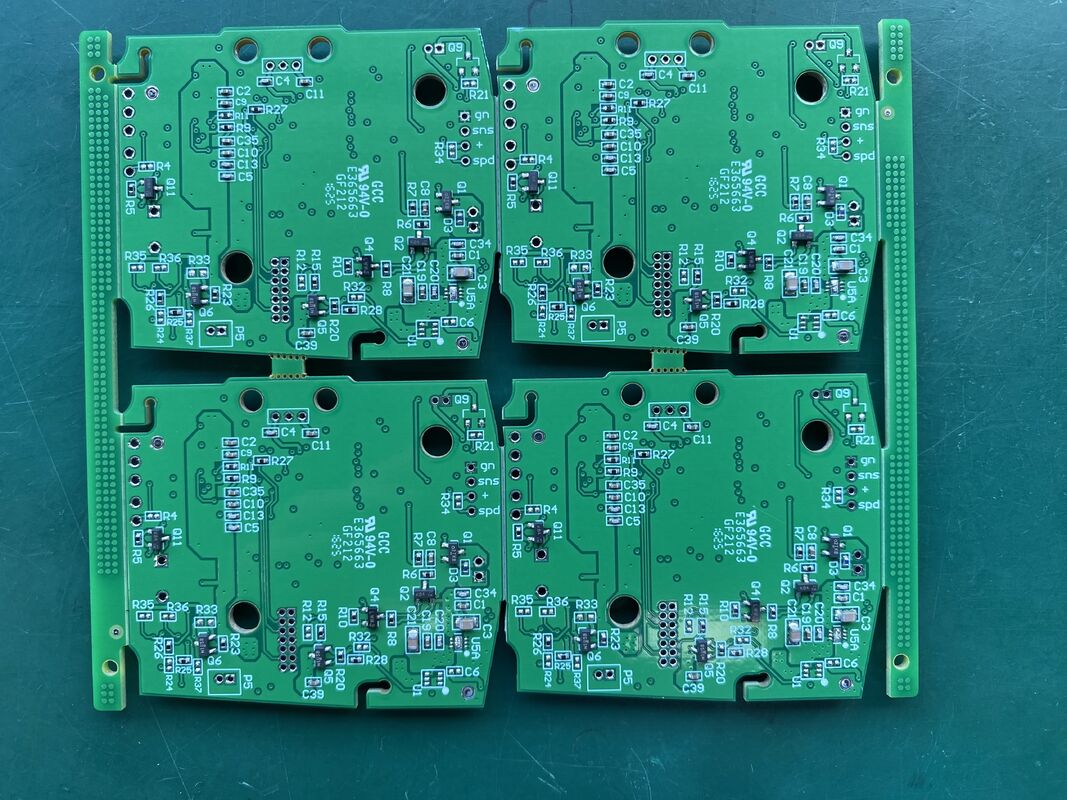
Product Description:
The Communication PCB Assembly is a highly specialized printed circuit board solution designed to meet the rigorous demands of modern communication systems. With a focus on precision, reliability, and customization, this product is engineered to support advanced electronic applications that require robust performance and exceptional signal integrity. The assembly incorporates a minimum hole diameter of 0.1mm, enabling intricate circuit designs and high-density component placement, which is essential for compact communication devices and systems.
One of the standout features of the Communication PCB Assembly is its comprehensive impedance control. This critical attribute ensures that signal transmission across the board is consistent and free from unwanted reflections or losses, which can degrade communication quality. Precise impedance management is vital for high-frequency applications, such as RF modules, wireless communication devices, and high-speed data transfer systems. By maintaining controlled impedance, the PCB assembly optimizes signal integrity and reduces electromagnetic interference, thereby enhancing overall system performance.
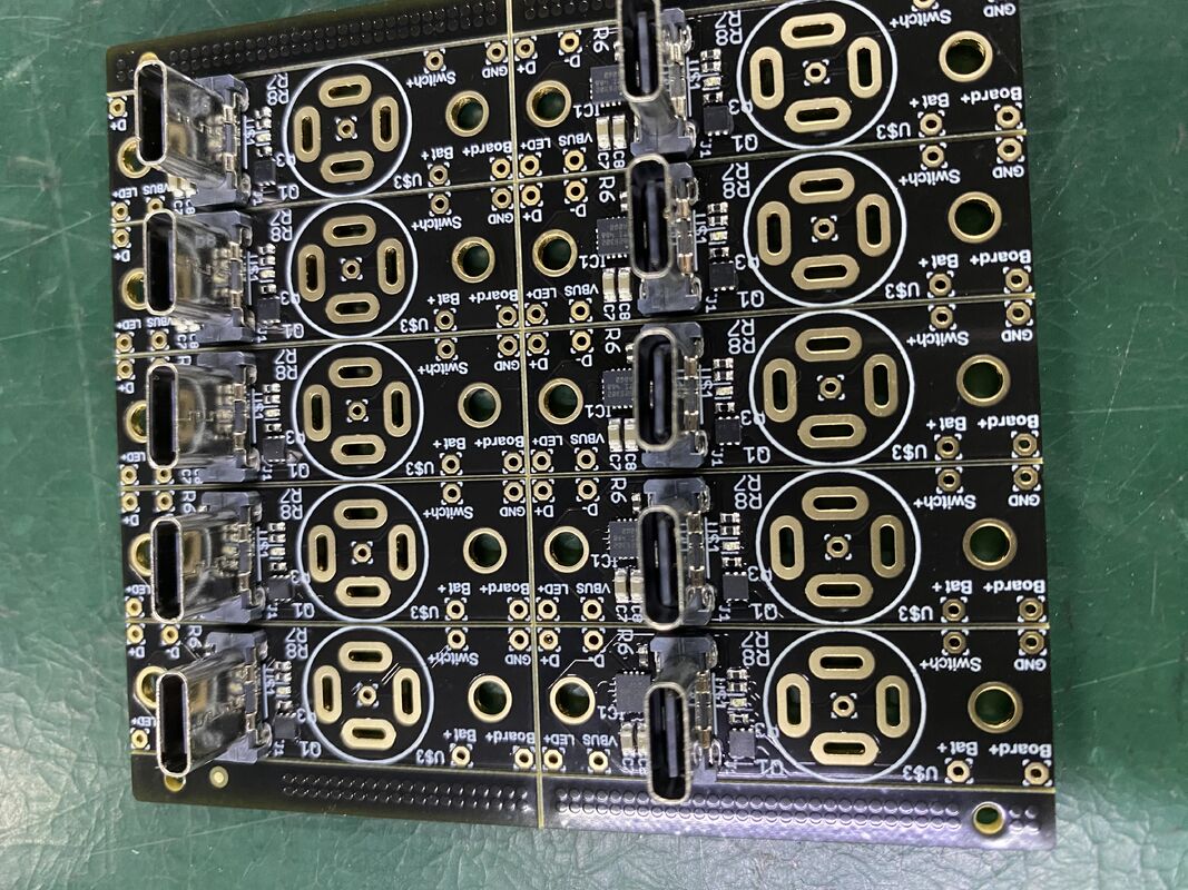
The design versatility of this Communication PCB Assembly is further enhanced by its support for multiple via types, including through-hole, blind, and buried vias. This flexibility allows for complex multilayer board configurations that maximize space utilization and electrical performance. Through-hole vias provide robust mechanical connections suitable for heavy current pathways, while blind and buried vias enable dense interconnects between inner layers without compromising surface real estate. Such advanced via technology is particularly beneficial in communication equipment where space constraints and electrical reliability are paramount.
Customization is a core aspect of this Communication PCB Assembly, allowing clients to tailor the product to their specific requirements. Whether it involves unique layer stack-ups, specialized materials, or precise electrical characteristics, the assembly can be adapted to meet diverse application needs. This bespoke approach ensures that the final product aligns perfectly with the intended operational environment and functional demands, offering a competitive edge in the rapidly evolving communications market.
Incorporating thick copper layers is another key feature of this PCB assembly, which significantly enhances its current-carrying capacity. Thick copper traces are essential for handling heavy current loads, making the assembly suitable for power-intensive communication devices and systems. The robustness provided by thick copper also improves thermal management, reducing the risk of overheating and extending the lifespan of the PCB. This attribute is especially important in high-reliability communication infrastructure where sustained performance under heavy electrical loads is critical.
Moreover, the Communication PCB Assembly is designed with built-in surge protection capabilities. Communication systems are often vulnerable to electrical surges caused by lightning strikes, power fluctuations, or electrostatic discharge. Integrating surge protection directly into the PCB assembly safeguards sensitive electronic components, preventing damage and ensuring uninterrupted operation. This feature enhances the durability and reliability of communication equipment deployed in harsh or unpredictable environments.
Overall, the Communication PCB Assembly offers a comprehensive solution for high-performance communication electronics. Its combination of fine hole diameter precision, advanced impedance control, versatile via structures, customizable options, thick copper layers for heavy current handling, and integrated surge protection makes it an ideal choice for manufacturers and designers aiming to deliver cutting-edge communication products. Whether used in telecommunications infrastructure, wireless devices, or data transmission systems, this assembly provides the foundation for reliable, efficient, and durable electronic communication solutions.
Features:
- Product Name: Communication PCB Assembly
- Minimum Hole Diameter: 0.1mm
- Via Types: Through Hole, Blind, Buried
- Specification: PCB Customized Size
- Communication PCB: High Tg170 and High Tg180
- Solder Mask Color Options: Blue, Green, etc.
- Thick Copper Layers for Enhanced Durability
- Surge Protection Features Integrated
- Designed for Heavy Current Applications
Technical Parameters:
| Product Name |
Communication PCB Assembly |
| Application Field |
5G Communication |
| Specification |
PCB Customized Size |
| Customized |
Yes |
| Viatype |
Through Hole, Blind, Buried |
| Min Hole Diameter |
0.1mm |
| Impedance Control |
Yes |
| Communication PCB |
High Tg170 And High Tg180 |
| Surface Finishing |
ENIG, HASL Lead Free |
| PCB Board |
HDI PCB |
Applications:
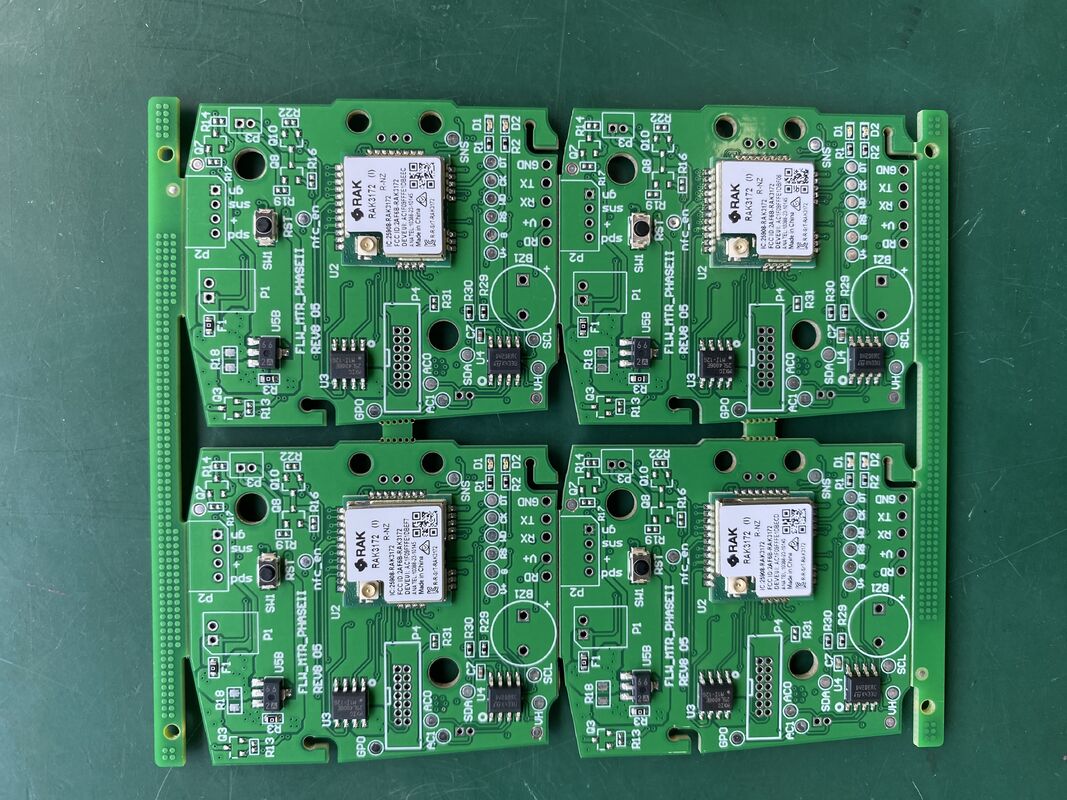
The Communication PCB Assembly is a highly specialized product designed for advanced applications in the field of 5G communication. As a Manufacturer committed to quality and innovation, we utilize high Tg170 and high Tg180 materials to ensure superior thermal stability and reliability under demanding operational conditions. This makes our Communication PCB Assembly ideal for use in environments where consistent performance is critical, such as telecommunications infrastructure and data transmission systems.
One of the primary application occasions for this Communication PCB Assembly is in 5G base stations and communication hubs. The high-density interconnect (HDI) PCB board technology incorporated in our design supports complex circuitry and miniaturization, which are essential for meeting the high-speed data requirements of 5G networks. Additionally, the impedance control feature embedded in the PCB assembly is crucial for maintaining signal integrity and minimizing losses, ensuring efficient and stable communication performance.
Surge protection is another key scenario where this Communication PCB Assembly excels. In communication systems, sudden voltage spikes can damage sensitive components, leading to system failures. Our PCB assemblies are designed with robust surge protection capabilities, safeguarding communication devices against unexpected electrical surges. This makes them indispensable in outdoor communication equipment and critical network components where reliability and durability are paramount.
The outer packaging of the Communication PCB Assembly is carefully designed using sturdy cartons, providing secure protection during transportation and storage. This packaging ensures that the PCBs remain free from physical damage, moisture, and static electricity, preserving their quality from the Manufacturer to the end user.
In summary, the Communication PCB Assembly finds its application in multiple scenarios including 5G communication infrastructure, surge protection systems, and any high-frequency communication equipment requiring HDI PCB technology with precise impedance control. As a trusted Manufacturer, we deliver products that meet the rigorous demands of modern communication networks, ensuring high performance, durability, and reliability in every unit.
Customization:
Our Communication PCB Assembly product offers comprehensive customization services to meet the diverse needs of manufacturers in the heavy current industry. We specialize in producing high-quality PCBs with various via types including Through Hole, Blind, and Buried vias, ensuring optimal electrical performance and reliability.
Manufacturers can benefit from our strict adherence to the ROHS PCB quality system, guaranteeing environmentally friendly and safe products. The board thickness can be customized from 0.2mm up to 6mm, allowing for versatile applications and enhanced durability in communication devices.
We provide a range of solder mask color options such as blue, green, and others to match your design requirements and improve the visual appeal of your PCBs. Each board is carefully packaged in sturdy cartons to ensure safe delivery and protection during transportation.
Choose our Communication PCB Assembly customization services for reliable manufacturing solutions tailored to support heavy current applications with superior quality and precision.
Support and Services:
Our Communication PCB Assembly product is supported by a dedicated technical support team committed to ensuring optimal performance and reliability. We provide comprehensive troubleshooting assistance, firmware updates, and configuration guidance to help you integrate and maintain your communication systems efficiently.
In addition to technical support, we offer a range of professional services including custom PCB design consultation, prototype development, testing and validation, as well as repair and refurbishment services. Our experts work closely with you to tailor solutions that meet your specific application requirements and industry standards.
We also provide detailed documentation, including user manuals, installation guides, and application notes to facilitate seamless deployment and operation of our Communication PCB Assembly products. Our goal is to empower you with the knowledge and tools necessary for successful implementation and long-term support.
Packing and Shipping:
Our Communication PCB Assembly products are carefully packaged to ensure maximum protection during transit. Each assembly is securely placed in anti-static bags to prevent electrostatic discharge, followed by cushioned packaging materials to absorb shocks and vibrations.
The packages are clearly labeled with handling instructions and product information to facilitate safe and efficient shipping. We use sturdy, high-quality boxes that comply with international shipping standards.
For shipping, we partner with reliable carriers to provide timely delivery and tracking services. We offer various shipping options to meet customer requirements, including expedited and standard delivery.
Upon receipt, customers are advised to inspect the packaging and product condition immediately and report any damages to ensure prompt resolution.


 Your message must be between 20-3,000 characters!