Product Description:
The Communication PCB Assembly is a highly specialized product designed to meet the rigorous demands of the modern 5G communication industry. As a leading manufacturer in the field, we pride ourselves on delivering top-quality printed circuit board assemblies that ensure exceptional performance, reliability, and durability. This product is specifically engineered to support the complex requirements of 5G communication systems, making it an essential component for cutting-edge telecommunications infrastructure.
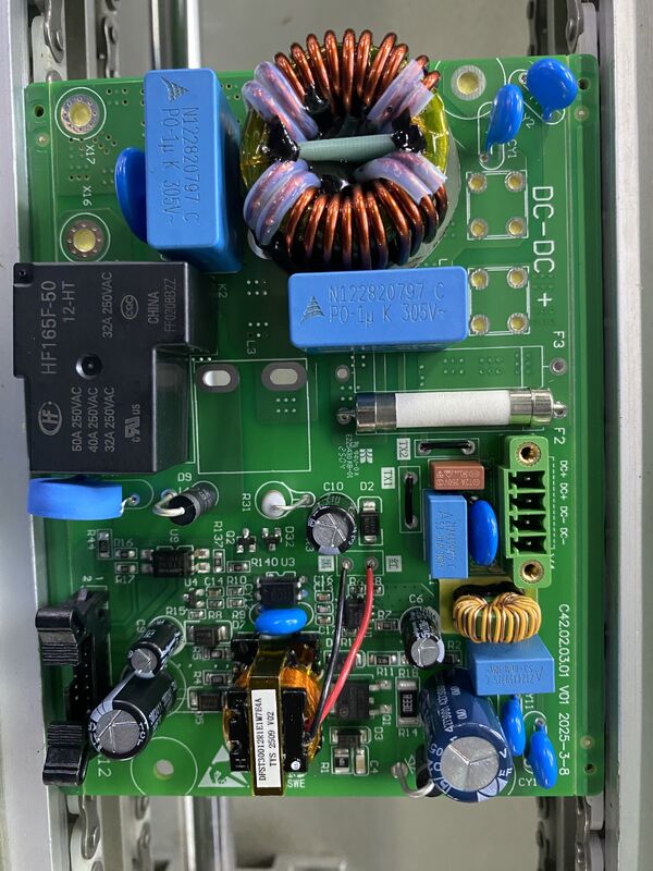
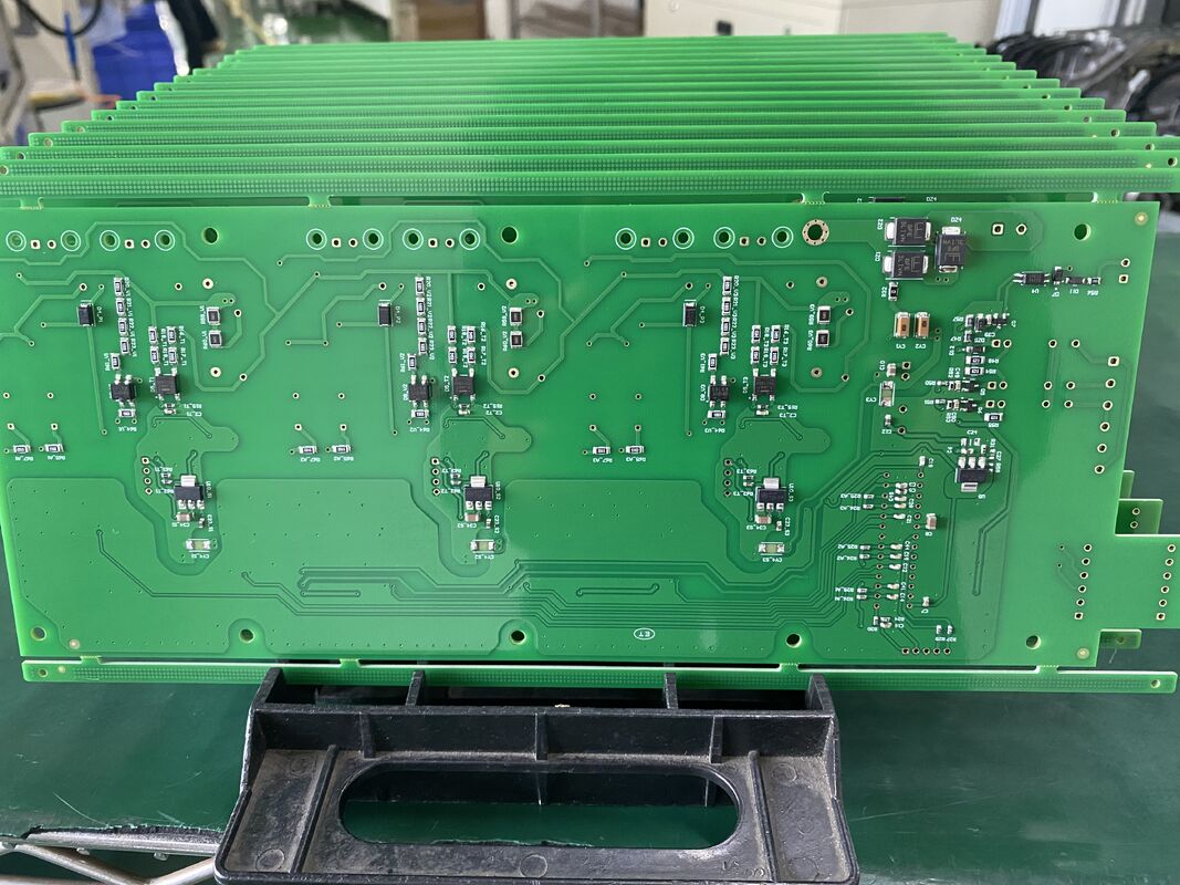
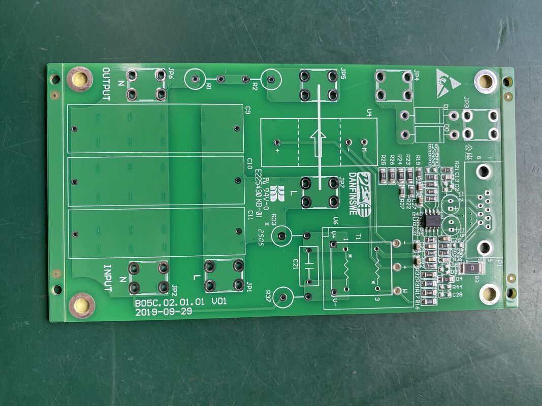
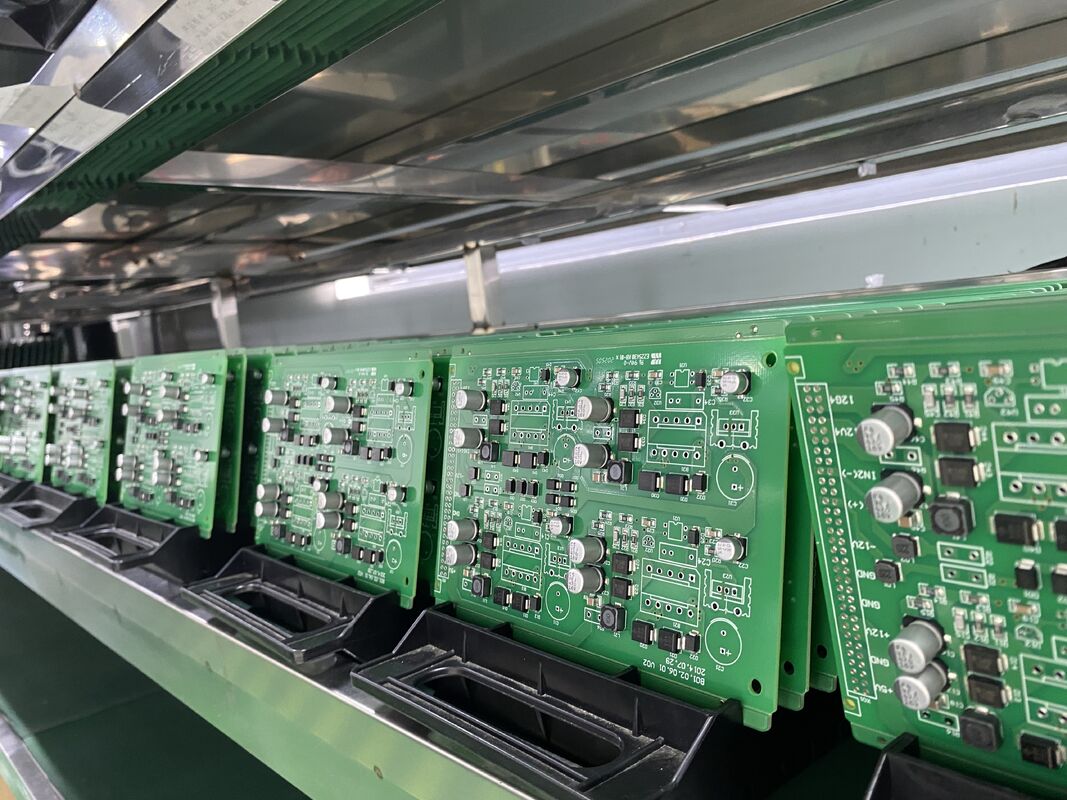
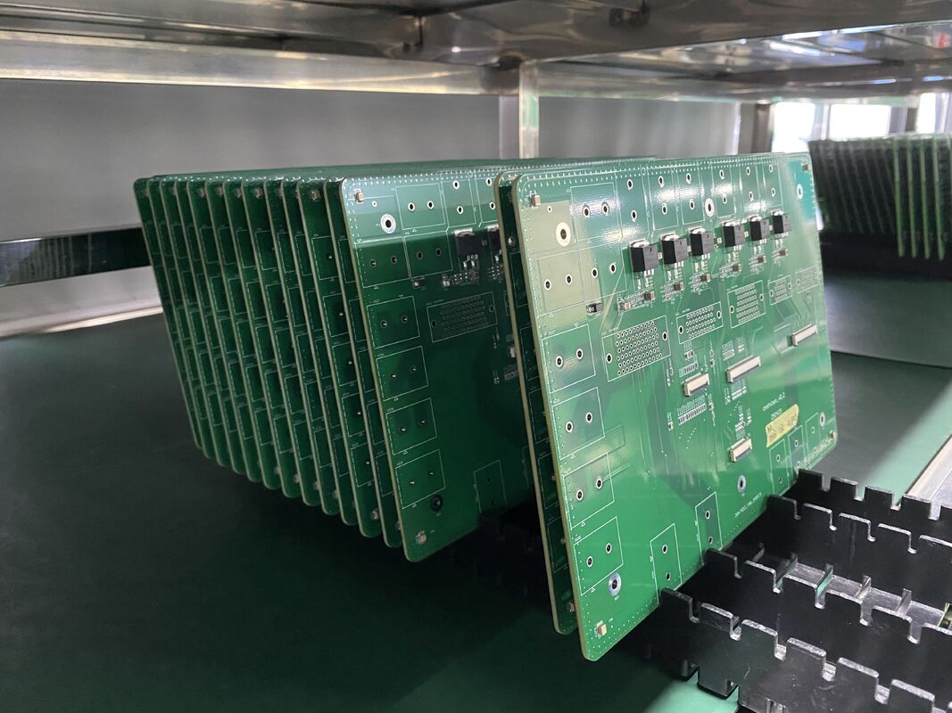
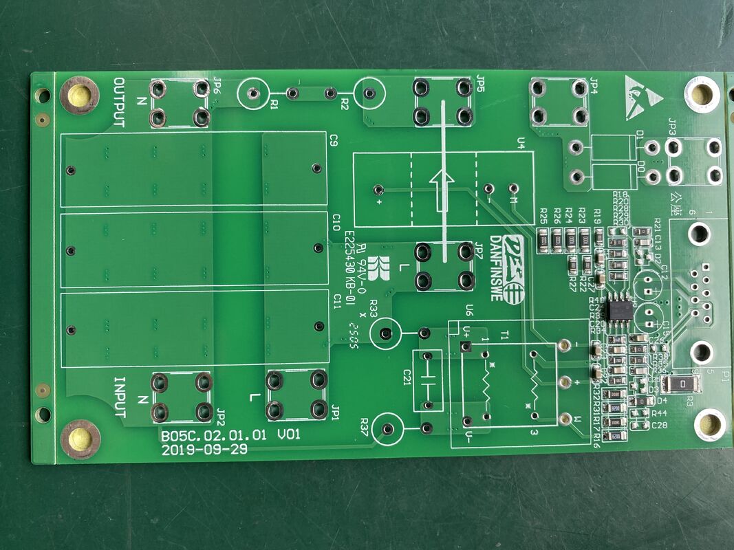
One of the standout features of our Communication PCB Assembly is its versatility in via types. It incorporates through hole, blind, and buried vias, enabling optimal electrical connectivity and signal integrity across multiple layers of the PCB. This multi-via configuration is crucial in managing the dense circuitry and high-frequency signals characteristic of 5G communication technology. The ability to utilize these varied via types also enhances the mechanical strength and thermal management of the assembly, ensuring long-lasting operation even under demanding conditions.
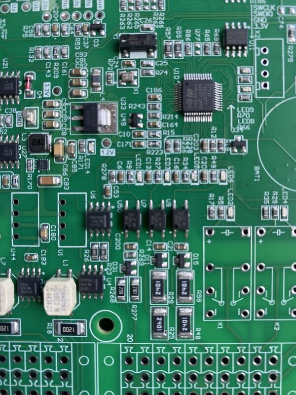
Precision is a hallmark of this assembly, with a minimum hole diameter of just 0.1mm. This fine detail allows for intricate circuit designs and high-density component placement, which are vital in the compact and complex layouts required by modern communication devices. The small hole diameter also contributes to improved signal transmission and reduced electromagnetic interference, which are critical factors in maintaining the high data rates and low latency that 5G networks demand.
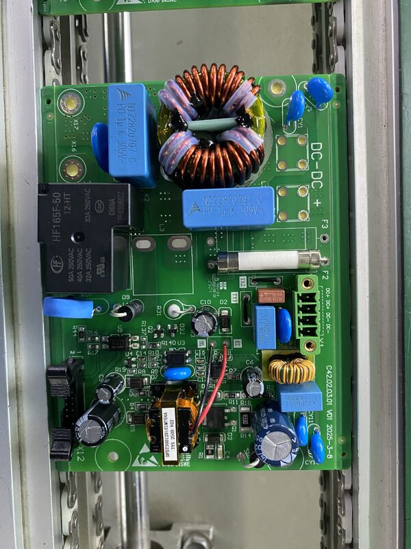
In terms of application, the Communication PCB Assembly is perfectly suited for the 5G communication field. It supports various devices and systems that rely on rapid data transfer and robust connectivity, including base stations, network infrastructure, and user equipment. The assembly's design ensures that it can handle the heavy current loads often encountered in these applications, providing stable and reliable power delivery without compromising performance.
Our commitment to quality extends to the packaging of the Communication PCB Assembly. Each unit is carefully packaged in a sturdy carton, ensuring protection during transportation and storage. This outer packaging safeguards the delicate components from environmental factors such as moisture, dust, and mechanical shock, preserving the integrity of the assembly until it reaches the end user.
As a manufacturer with extensive experience in the electronics industry, we understand the importance of delivering products that meet both technical specifications and industry standards. The Communication PCB Assembly undergoes rigorous testing and quality control processes to guarantee compliance and optimal functionality. This dedication to excellence ensures that our customers receive a product that not only meets but exceeds expectations in performance and reliability.
Moreover, the design and manufacturing process of this PCB assembly take into account the need for handling heavy current applications. The robust construction and carefully selected materials enable the assembly to manage substantial electrical loads without overheating or failure. This capability is especially important in 5G communication systems, where power efficiency and thermal management are critical for maintaining network stability and longevity.
In summary, the Communication PCB Assembly is a state-of-the-art product tailored for the evolving demands of 5G communication technology. Its combination of through hole, blind, and buried vias, along with a minimum hole diameter of 0.1mm, makes it ideal for sophisticated circuit designs and high-frequency signal transmission. Packaged securely in a carton for maximum protection, this assembly is engineered to support heavy current applications reliably. As a trusted manufacturer, we deliver a product that embodies quality, precision, and durability, ensuring optimal performance in the fast-paced world of 5G communications.
Features:
- Product Name: Communication PCB Assembly
- Communication PCB: High Tg170 and High Tg180 for enhanced durability
- Specification: PCB Customized Size to meet specific project requirements
- Surface Finishing: ENIG and HASL Lead Free for superior conductivity and environmental compliance
- Via Type: Through Hole, Blind, and Buried vias for complex circuit designs
- Ideal for Communication Infrastructure applications
- Reliable Manufacturer specializing in high-quality Communication PCB Assembly
Technical Parameters:
| Product Name |
Communication PCB Assembly |
| PCB Quality System |
ROHS |
| Solder Mask Color |
Blue, Green, Etc. |
| Via Type |
Through Hole, Blind, Buried |
| Application Field |
5G Communication |
| Surface Finishing |
ENIG, HASL Lead Free |
| PCB Layers |
6 Layers |
| Communication PCB |
High Tg170 and High Tg180 |
| Specification |
PCB Customized Size |
| Customized |
Yes |
Applications:
The Communication PCB Assembly, designed with advanced HDI PCB technology, is an essential component in modern communication infrastructure. Featuring a compact 6-layer PCB structure, this product ensures high-density interconnections and exceptional signal integrity, making it ideal for complex electronic systems used in 5G communication networks. The assembly’s minimum hole diameter of 0.1mm allows for precise and reliable connections, which are critical for maintaining the high-speed data transmission required in next-generation communication systems.
In the realm of 5G communication, the demand for robust and efficient communication infrastructure has never been greater. This Communication PCB Assembly meets these demands by utilizing high Tg materials, specifically High Tg170 and High Tg180, which provide superior thermal stability and mechanical strength. These attributes enable the PCB to withstand the heat generated by heavy current loads, ensuring consistent performance and longevity in demanding environments.
This product is particularly suited for application occasions where high-frequency signal transmission and durability under heavy current conditions are crucial. It finds extensive use in base stations, signal repeaters, and network routers that form the backbone of 5G communication infrastructure. The combination of HDI technology and high Tg materials makes it capable of supporting the rigorous operational requirements of these devices, which often operate continuously under heavy electrical loads.
Moreover, the Communication PCB Assembly is ideal for scenarios involving the deployment and maintenance of communication infrastructure in urban and rural areas alike. Its robust design and precise engineering allow it to perform reliably in various environmental conditions, ensuring uninterrupted communication services. This makes it a preferred choice for telecom operators aiming to expand and upgrade their networks with cutting-edge 5G technology.
In summary, the Communication PCB Assembly with its 6-layer HDI PCB, minimum hole diameter of 0.1mm, and use of High Tg170 and High Tg180 materials, is a critical enabler in the advancement of communication infrastructure. It supports heavy current applications within 5G communication systems, delivering the performance and reliability required for today’s fast-evolving communication landscape.
Customization:
Our Communication PCB Assembly product offers comprehensive product customization services tailored to meet your specific requirements. As a leading manufacturer, we ensure that every PCB assembly complies with the ROHS quality system, guaranteeing environmentally friendly and reliable performance. We specialize in HDI PCB boards, allowing for high-density interconnections that optimize your communication devices. Our manufacturer expertise includes advanced viatype options such as Through Hole, Blind, and Buried vias, providing enhanced electrical performance and design flexibility. Partner with our manufacturer team to customize your Communication PCB Assembly with precision and quality you can trust.
Support and Services:
Our Communication PCB Assembly product is backed by comprehensive technical support and services to ensure optimal performance and reliability. We provide expert guidance throughout the entire lifecycle of the product, from initial design consultation to post-deployment maintenance.
Our technical support team is equipped to assist with troubleshooting, firmware updates, and system integration to help you achieve seamless communication solutions. We also offer detailed documentation, including user manuals, installation guides, and configuration instructions to facilitate easy setup and operation.
In addition, we provide custom testing and quality assurance services to meet specific project requirements and industry standards. Our commitment to continuous improvement ensures that you receive timely updates and enhancements to keep your communication systems running efficiently.
Whether you need assistance with assembly specifications, performance optimization, or compatibility issues, our dedicated support staff is available to provide prompt and effective solutions tailored to your needs.
Packing and Shipping:
Our Communication PCB Assembly products are carefully packaged to ensure maximum protection during transit. Each assembly is securely placed in anti-static bags to prevent electrostatic discharge, followed by cushioned packaging materials to absorb shocks and vibrations.
The assemblies are then packed in sturdy, double-walled corrugated boxes designed to withstand handling and shipping stresses. For larger orders, we use custom-fit foam inserts or trays to keep each PCB securely in place and prevent movement within the box.
All packages are clearly labeled with handling instructions, including “Fragile” and “Handle with Care” warnings, to ensure proper treatment throughout the shipping process.
We offer multiple shipping options based on customer requirements, including expedited and standard delivery services. Our logistics partners are selected for their reliability and experience in handling sensitive electronic components, ensuring that your Communication PCB Assemblies arrive on time and in perfect condition.
Additionally, tracking information is provided for all shipments, allowing customers to monitor the progress of their orders from our facility to their doorstep.


 Your message must be between 20-3,000 characters!