Product Description:
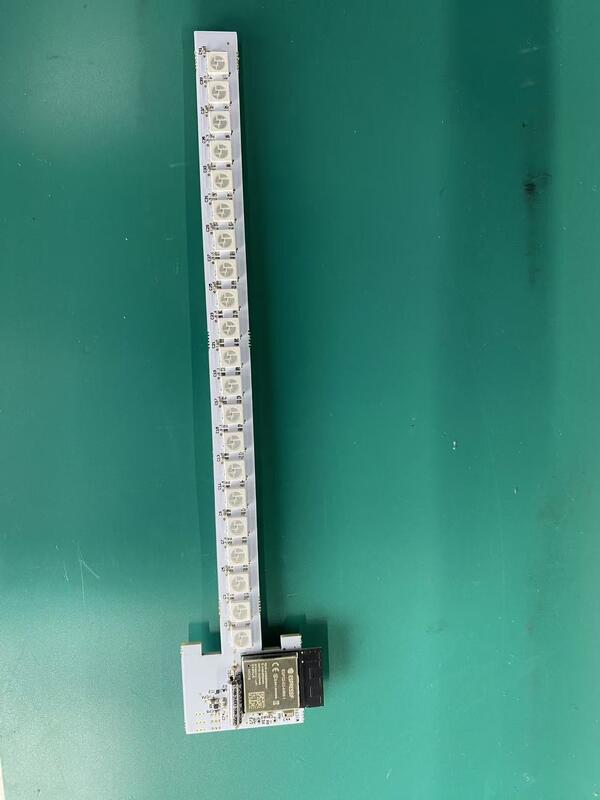
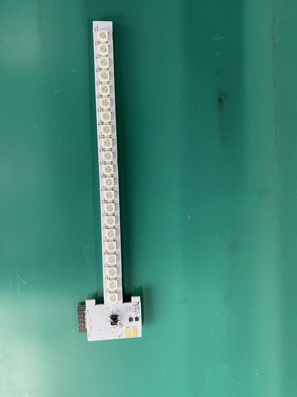
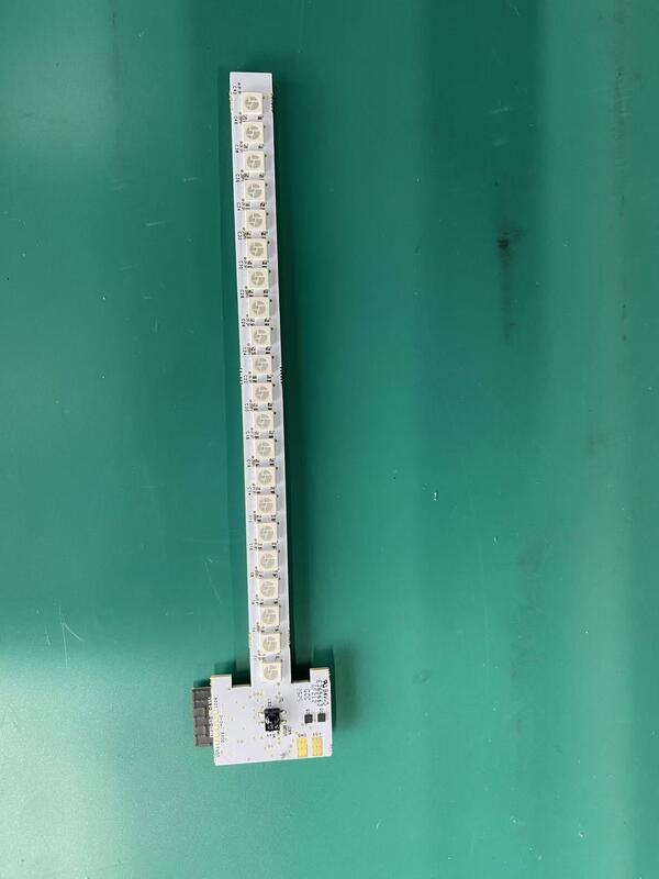
The Communication PCB Assembly is a highly advanced and reliable printed circuit board solution designed specifically for modern communication infrastructure. As a critical component in the telecommunications industry, this product is engineered to meet the rigorous demands of high-speed data transmission and complex signal processing. Manufactured with precision and expertise, the Communication PCB Assembly ensures optimal performance, durability, and efficiency in various communication devices and systems.
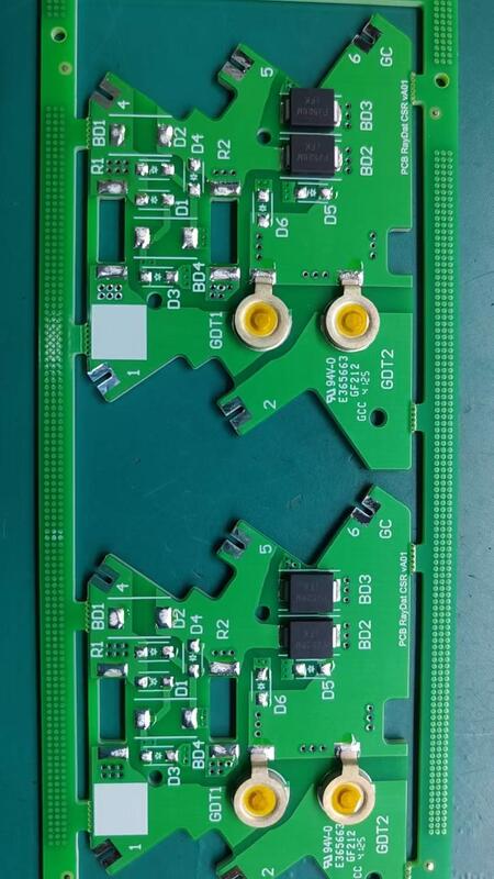
One of the standout features of this Communication PCB Assembly is its 6-layer PCB configuration. The multi-layer design allows for enhanced circuit density and improved electrical performance, making it ideal for complex communication applications. By providing multiple signal layers, power planes, and ground planes, the 6-layer structure minimizes electromagnetic interference and crosstalk, which are crucial factors in maintaining signal integrity in communication infrastructure.
Impedance control is another vital attribute of this Communication PCB Assembly. Proper impedance matching is essential in high-frequency circuits to ensure signal integrity and reduce signal loss or reflection. The manufacturer implements precise impedance control techniques during the PCB fabrication process, which helps maintain consistent electrical characteristics throughout the board. This is particularly important in communication systems where signals travel at high speeds and any impedance mismatch can lead to data errors or reduced performance.
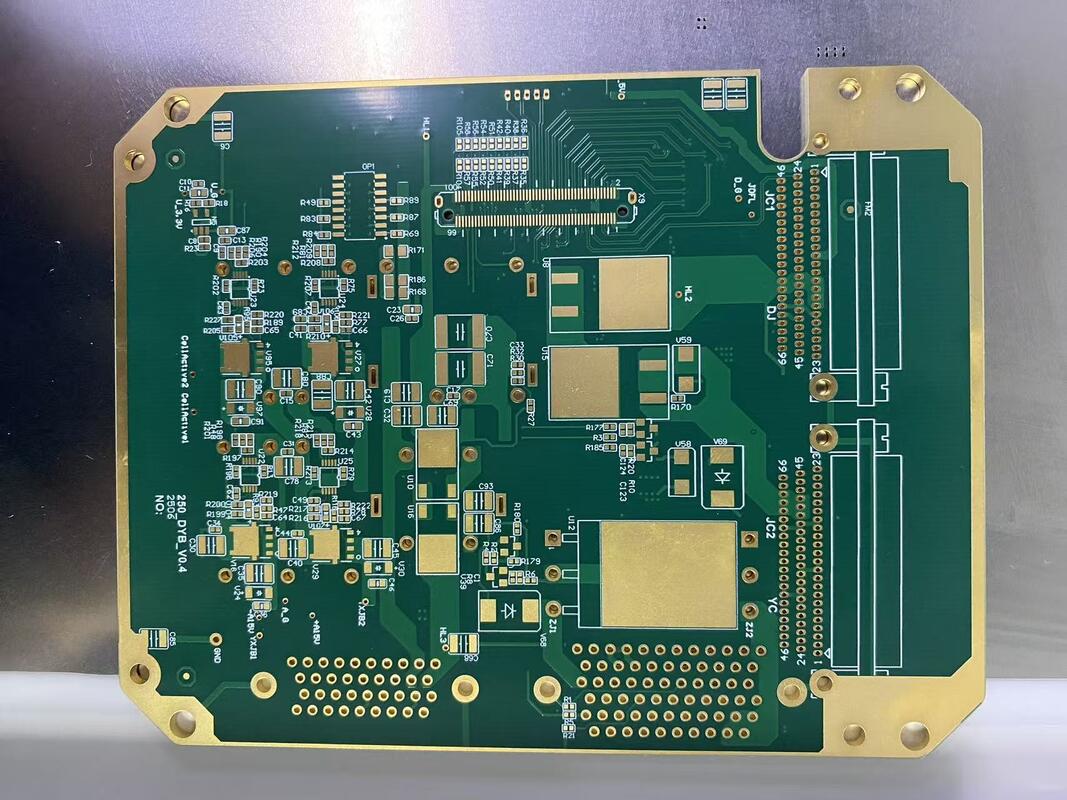
This Communication PCB Assembly utilizes HDI (High-Density Interconnect) PCB technology, a cutting-edge approach that enhances circuit density while maintaining a compact form factor. HDI PCBs incorporate microvias, blind and buried vias, and fine lines to achieve greater component density and shorter signal paths. This technology is indispensable for communication devices that require miniaturized boards without compromising functionality or performance. The HDI PCB used in this assembly allows for efficient routing and better electrical performance, making it an ideal choice for advanced communication equipment.
The product features a minimum hole diameter of 0.1mm, which exemplifies the precision and advanced manufacturing capabilities of the manufacturer. Such small via sizes enable the creation of intricate circuit designs with high component density, allowing the Communication PCB Assembly to support complex layouts and multi-layer interconnections. This level of detail is critical for modern communication devices that demand compactness, reliability, and high-speed operation.
Moreover, the Communication PCB Assembly incorporates thick copper layers to enhance current carrying capacity and improve thermal management. Thick copper is essential in communication infrastructure, where boards may need to handle higher power levels and dissipate heat efficiently. The use of thick copper also contributes to the mechanical strength and durability of the PCB, ensuring long-term reliability even in harsh operating environments.
As a trusted manufacturer of Communication PCB Assemblies, the company leverages state-of-the-art fabrication processes and rigorous quality control measures to deliver products that meet industry standards and customer specifications. The combination of 6-layer PCB design, impedance control, HDI technology, small hole diameters, and thick copper layers results in a superior product that supports the demanding needs of modern communication systems.
In summary, the Communication PCB Assembly is an advanced, high-performance solution tailored for the communication infrastructure sector. Its 6-layer HDI PCB design with impedance control ensures excellent electrical performance, while the small hole diameter and thick copper layers provide enhanced reliability and durability. Manufactured with precision and expertise, this product stands out as a dependable choice for communication equipment manufacturers seeking to achieve optimal functionality and efficiency in their devices.
Features:
- Product Name: Communication PCB Assembly
- PCB Layers: 6 Layers for enhanced circuit density and performance
- Outer Package: Durable Carton packaging ensuring safe delivery
- Communication PCB: High Tg170 and High Tg180 materials for superior thermal stability
- Specification: PCB Customized Size to meet specific design requirements
- PCB Quality System: ROHS compliant, ensuring environmentally friendly manufacturing
- Thick copper layers enabling Heavy Current capacity for robust electrical performance
- Integrated surge protection features for enhanced reliability and safety
Technical Parameters:
| Product Name |
Communication PCB Assembly |
| Manufacturer |
Communication infrastructure |
| Specification |
PCB Customized Size |
| Customized |
Yes |
| Solder Mask Color |
Blue, Green, etc. |
| Min Hole Diameter |
0.1mm |
| Application Field |
5G Communication |
| PCB Quality System |
ROHS |
| PCB Board |
HDI PCB |
| Impedance Control |
Yes |
| Outer Package |
Carton |
| Heavy Current |
Supported |
Applications:
The Communication PCB Assembly is a highly reliable and efficient solution designed to meet the demanding requirements of modern communication systems. Manufactured under strict quality controls and compliant with the ROHS standards, this PCB assembly ensures environmentally friendly production without compromising performance. The 6-layer PCB structure provides enhanced signal integrity and optimal electrical performance, making it ideal for complex communication devices that require multi-layer routing and effective noise reduction.
One of the key features of this Communication PCB Assembly is its thick copper layers, which significantly improve current carrying capacity and thermal management. Thick copper is essential in communication equipment where high power and high-frequency signals are prevalent. This attribute ensures durability and stable performance even under rigorous operating conditions, making it suitable for use in base stations, routers, and other network infrastructure components.
The surface finishing options, including ENIG (Electroless Nickel Immersion Gold) and HASL Lead-Free, provide excellent solderability and corrosion resistance. These finishes are crucial for maintaining long-term reliability and consistent electrical contact in communication devices that often operate in various environmental conditions. Additionally, the impedance control feature embedded in the PCB design ensures signal integrity and reduces signal loss, which is vital for high-speed data transmission and minimizing electromagnetic interference in communication systems.
From a packaging perspective, the Communication PCB Assembly is carefully packed in sturdy cartons that protect the product during transit and storage. This packaging approach safeguards the PCB from physical damage, moisture, and dust, ensuring that the product arrives in perfect condition ready for immediate integration into communication equipment.
Manufacturers looking for robust and high-performance PCBs for applications such as telecommunications infrastructure, satellite communication devices, wireless communication modules, and data communication systems will find this Communication PCB Assembly an ideal choice. Its combination of thick copper layers, multi-layer design, ROHS compliance, and precise impedance control makes it a dependable component for cutting-edge communication technology.
In summary, this Communication PCB Assembly is perfectly suited for a variety of application occasions and scenarios including 5G base stations, fiber optic communication devices, IoT communication modules, and enterprise networking hardware. Its advanced features and quality standards ensure that it can withstand the challenges of high-frequency, high-power communication environments, providing manufacturers with a reliable and efficient PCB solution.
Customization:
Our Communication PCB Assembly product offers comprehensive customization services tailored to meet the demanding requirements of 5G communication applications. We provide a variety of solder mask color options, including blue, green, and others, to suit your specific design preferences. The PCB boards are manufactured using advanced HDI PCB technology, ensuring high-density interconnections and superior performance.
We specialize in precise impedance control to optimize signal integrity, which is critical for high-speed 5G communication systems. The board thickness can be customized within the range of 0.2-6mm to accommodate different mechanical and electrical needs. Additionally, our PCBs are designed with thick copper layers to support heavy current loads and enhance surge protection, ensuring reliable operation under demanding conditions.
With our product customization services, you can expect high-quality communication PCB assemblies that deliver durability, efficiency, and excellent electrical performance tailored specifically for 5G communication environments.
Support and Services:
Our Communication PCB Assembly product is backed by comprehensive technical support and services to ensure optimal performance and reliability. We provide expert guidance throughout the entire lifecycle of the product, from design and prototyping to manufacturing and deployment.
Our technical support team is available to assist with troubleshooting, firmware updates, and customization requests to meet specific communication requirements. We also offer detailed documentation, including datasheets, assembly instructions, and application notes to facilitate seamless integration into your systems.
In addition, we provide testing and quality assurance services to guarantee that each PCB assembly meets stringent industry standards and customer specifications. Our commitment to excellence ensures minimal downtime and maximum efficiency for your communication solutions.
For ongoing maintenance and upgrades, we offer tailored service plans to keep your Communication PCB Assembly operating at peak performance. Trust our dedicated support team to deliver timely and effective solutions to any technical challenges you may encounter.
Packing and Shipping:
Our Communication PCB Assembly products are carefully packaged to ensure maximum protection during transit. Each assembly is placed in anti-static bags to prevent electrostatic discharge, followed by cushioning materials to safeguard against mechanical shocks and vibrations. The packaging is designed to maintain the integrity and functionality of the PCB throughout handling and shipping.
For shipping, we use sturdy, high-quality cartons that are clearly labeled with handling instructions and product information. We offer multiple shipping options to meet your delivery timeline requirements, including express and standard services. All shipments are tracked to provide real-time updates and ensure timely delivery of your Communication PCB Assembly products.


 Your message must be between 20-3,000 characters!