Suntek Group is a leading supplier in EMS field with one-stop solution for PCB/FPC
assembly,Cable assembly,Mix technology assembly and Box-buildings.
Suntek Electronics Co., Ltd,as the major facility, located in Hunan Prov,China;
BLSuntek Electronics Co., Ltd,as the new facility,located in Kandal Prov,Cambodia.
Capabilities overview:
| Layers: |
Rigid PCB 2 - 40 + Layers, Rigid-flex PCB 1 - 10Layers |
| Panel Size(max): |
21" x 24" |
| PCB Thickness: |
0.016" to 0.120" |
| Line & Spaces: |
0.003" / 0.003" Inner Layers; 0.004" Outer Layers |
| Hole Size: |
0.006" Thru Hole (Finished Size) and 0.004" Buried Via |
| Materials: |
FR4, High Tg, Rogers, Halogen-free material, Teflon, Polyimide |
| Surface Finishes: |
ENi/IAu, OSP, Lead-free HASL,Immersion Gold/Silver, Immersion Tin |
| Special Products: |
Blind/ Buried Via(HDI 2+N+2), Rigid Flex |
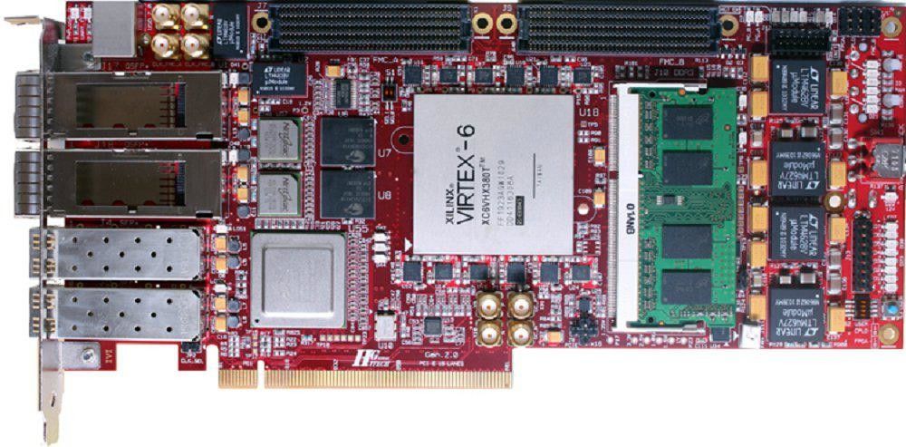
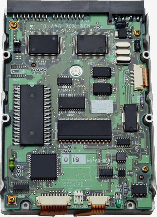
Applications and Types of PCBs for Telecommunications Industry
PCBs are a necessity for the telecommunications industry. From a PCB for broadcasting networks to PCBs for office communications, printed circuit boards are what makes electronic communications equipment possible. It's hard to imagine how we communicated at all before the advent today's sophisticated communication technology.
Thanks to that equipment and the communication PCBs that reside within, we can connect to each other faster, more clearly and more efficiently than ever before. Of course, to enjoy that clear, fast, effective communication, we need the right telecom printed circuit boards for the job.
Communication is the most important downstream application field of PCB. PCB has a wide range of applications in various aspects such as wireless network, transmission network, data communication and fixed network broadband, and it is usually added value such as backplane, high-frequency high-speed board, and multi-layer PCB board. Higher product. 5G is the next generation mobile communication network, and there will be a large amount of infrastructure construction demand by then, which is expected to greatly boost the demand for communication boards.
Here are the most common applications of the telecommunication industry that make efficient use of PCBs:
- Wireless communication systems
- Mobile phone tower systems
- Telephonic switching systems
- PBX systems
- Industrial wireless communication technology
- Technology for commercial phones
- Video conferencing technologies
- Communication technology used in space
- Cell transmission and tower electronics
- High speed servers and routers
- Electronic data storage devices
- Mobile communication systems
- Satellite systems and communication devices
- Video collaboration systems
- Land wired communication systems
- Technology for commercial phones
- Digital and analog broadcasting systems
- Voice over Internet Protocol (VoIP)
- Signal boost systems (online)
- Security technology and information communication systems
Our supports
We ensure cost transparency, BOM cost breakdown sharing
We have components suppliers from the Global.
We have a written process to advise customers of any schdule delays or product quality problems,by:
(1)Customer service procedure
(2)RMA procedure
(3)8D reports
(4)PDCA(Plan-Do-Check-Action) in customer service
We respond to the complaints,issues and queries in 24 hours, by:
(1) Weekly reports
(2) Customer supporting team to review communication times
(3) Customer satisfaction questionnaire
Aftersales services:
(1) 1-year guarantee period for all of products
(2) FOC repair
(3) Quick compensation parts to replace defectives.


 Your message must be between 20-3,000 characters!