Suntek Group is a leading supplier in EMS field with one-stop solution for PCB/FPC assembly,Cable assembly,Mix technology assembly and Box-buildings.
Suntek Electronics Co., Ltd,as the major facility, located in Hunan Prov,China;
BLSuntek Electronics Co., Ltd,as the new facility,located in Kandal Prov,Cambodia.With ISO9001:2015,ISO13485:2016,IATF 16949:2016 and UL E476377 certified,.We deliver qualified products with competitive price to clients all over the world.
We have 2 manufacturers, one in China ,other one in Cambodia.

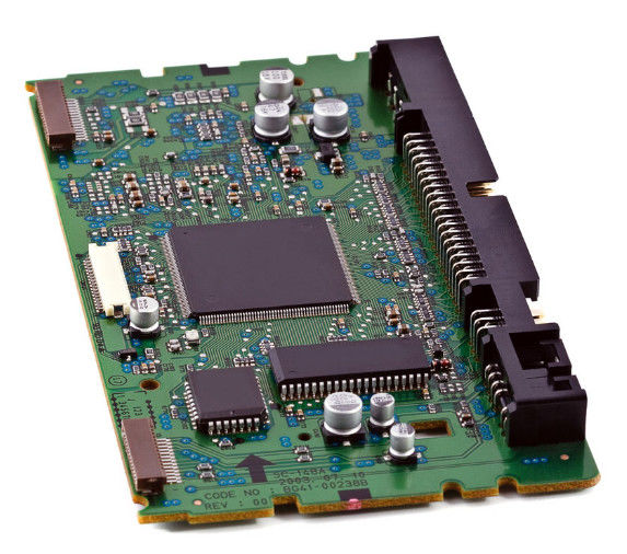
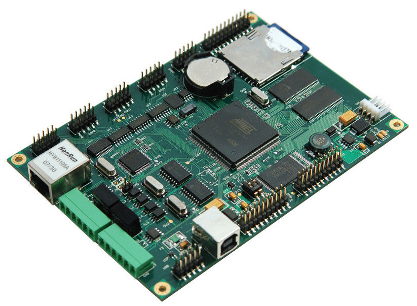
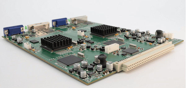
PCB-PCBA Application:
* Automobiles,Machinery
* Electronical machine,Projector
* Advertising machine,Monitor,Home appliance
* Water Dispensers,Computer,Motherboard
* Military equipment,Air conditioner
* Communications-equipment,Power device,etc.
FAQ:
Q1: What files do you use in PCB fabrication?
A1: Gerber, BOM,Drawings.
Q2: How do you make sure the quality?
A2: Our Product is all 100% E-tested .PCB Assembly are with 100% AOI,ICT,FT and Visual checking,100% X-ray for BGA.
Q3: Can we visit your company?
A3: Of course,Welcome to visit our company, Suntek located in Xingsha Industrial Park, Changsha,Hunan province, China.
Q4: What is the lead time?
A4: It takes 3-5 working days for sample, 7-10 working days for batch production based on files and quantity. It takes 15-20 working days for PCB assembly.
Q5: Will you keep our information and files secret?
A5: Sure,It is our basic principle to keep business secrets to protect our customers' designs.NDA can be signed at any time.
Q6. How to work with you?
A6: -Email and send us the PCB layout file, BOM list
- We will provide reply confirmation within 12 hours and reply to the offer within 3-5 days.
- Waiting for your company to confirm the price, order and payment terms.
- We will proceed the order.

 Your message must be between 20-3,000 characters!